A printed circuit board (PCB) consists of several distinct layers, each serving a specific purpose. Here are the primary layers of a PCB and their materials:
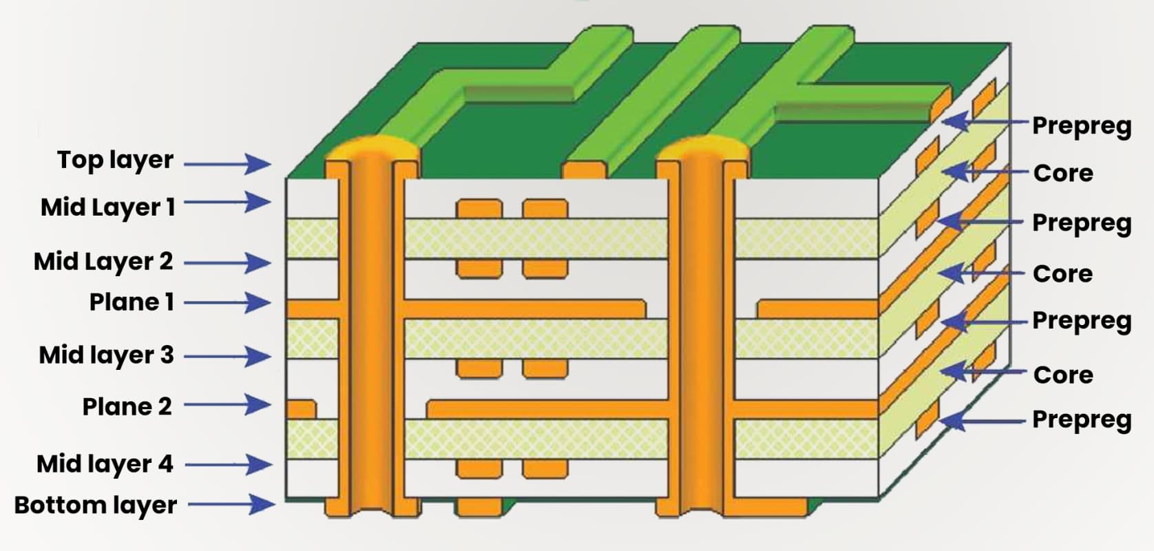
- Substrate/Core Layer:
- Material: Typically made of fiberglass (FR4) or other insulating material.
- Purpose: Provides mechanical support and the base structure of the PCB.
- Copper Layer:
- Material: Copper foil.
- Purpose: Forms the conductive pathways (traces) that connect different components.
- Solder Mask Layer:
- Material: Liquid photo-imageable (LPI) solder mask or epoxy-based resin.
- Purpose: Insulates the copper traces to prevent short circuits and protect against environmental damage.
- Silkscreen Layer:
- Material: Ink (usually white, but can be other colors).
- Purpose: Provides labeling and identification marks for components and test points.
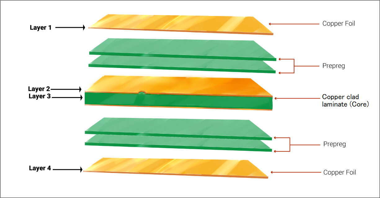
- Dielectric/Prepreg Layer:
- Material: Epoxy resin (often FR4) impregnated fiberglass.
- Purpose: Insulates different copper layers from each other and bonds them together during the lamination process.
- Copper Planes (Power/Ground Planes):
- Material: Copper foil.
- Purpose: Provides a stable voltage reference and helps in power distribution and signal integrity.
- Surface Finish Layer:
- Material: Various options like HASL (Hot Air Solder Leveling), ENIG (Electroless Nickel Immersion Gold), or OSP (Organic Solderability Preservatives).
- Purpose: Protects the exposed copper and provides a solderable surface for component attachment.